
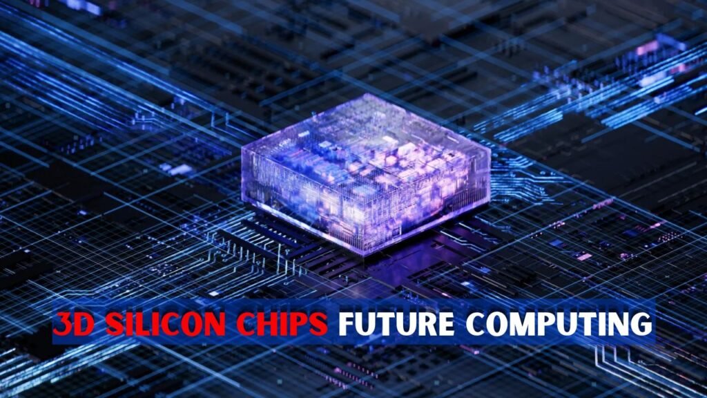
Monolithic 3D Silicon Chips Could Change Future Computing

Main Heading: How Monolithic 3D Chips Work
Monolithic 3D chips are constructed by stacking devices vertically, with insulating and wiring layers in between. It is not just a matter of taking two finished chips and glueing them together. Since the layers are manufactured on the same wafer, the vertical interconnects can be very small and very close together. These are inter-tier monolithical vias. They allowed signals to zip back and forth between logic and storage. The big plus is less data to move around. In modern computing, shuffling data around can consume more power than the computing itself. Monolithic 3D design can improve speed, bandwidth and power efficiency across the board by clustering related parts close together in a dense cluster.
 Samsung Introduces Flex Titanium Display Technology for Its Next Generation Foldable Phones
- It deposits active silicon layers on a wafer.
- Vertical inter-layer connections are small.
- It reduces on-chip path length.
- It may produce memory close to the logic units.
- This allows the chip to process data more efficiently.
Why They Matter for Future Computing
Monolithic 3D chips are constructed by stacking devices vertically, with insulating and wiring layers in between. It is not just a matter of taking two finished chips and glueing them together. Since the layers are manufactured on the same wafer, the vertical interconnects can be very small and very close together. These are inter-tier monolithical vias. They allowed signals to zip back and forth between logic and storage. The big plus is less data to move around. In modern computing, shuffling data around can consume more power than the computing itself. Monolithic 3D design can improve speed, bandwidth and power efficiency across the board by clustering related parts close together in a dense cluster.

- It deposits active silicon layers on a wafer.
- Vertical inter-layer connections are small.
- It reduces on-chip path length.
- It may produce memory close to the logic units.
Benefits for AI, Memory, and Energy
The AI computation is one of the most promising application of monolithic 3D chips. AI systems need quick access to memory and often waste energy moving data that’s not needed. Memory is close to logic so chip can feed data faster and delay less. That could mean better AI for training, inference, image recognition, language processing and edge devices. Energy savings also matter in data centres where the costs of electricity and cooling are high. This can enable higher bandwidths and lower power consumption at shorter signal paths. It lets users enjoy faster apps, longer battery life, smarter cameras and more powerful devices that can do complex tasks locally instead of sending data to remote cloud servers for every request.

Challenges Before Mass Adoption
Monolithic 3D silicon chips are promising, but they are not easy to build. The upper layers must be built at a low enough temperature not to damage the layers underneath. Heat is another big challenge, as stacked devices can trap heat inside the chip. Designers require trusted tools to test, fix and design circuits in multiple vertical layers. Yield is important too. If one layer has defects the whole chip can be expensive. But manufacturers have to prove they can mass-produce these chips safely and at large volumes. As solutions to these challenges evolve, monolithic 3D chips will first gain traction in niche markets before becoming widespread, especially in applications where performance improvements justify the higher risk and design investment required during early adoption.
Final Thought
Monolithic 3D silicon chips could revolutionise computing of the future by enabling denser, faster and more energy efficient chips. Their main advantage is less data movement between important areas such as memory and logic. This can help AI, mobile devices, servers and smart machines work better with less power.” Still, the technology must overcome heat, cost, design and manufacturing problems before it becomes commonplace. If these challenges can be overcome, monolithic 3D chips could be among the most important routes for the next generation of computing across many industries and in our everyday digital lives.